CE Certification China Suppliers Factory Ultra-Pure Water System for Semiconductor & Microelectronics Manufacturing - 18.2 MΩ·cm Resistivity Suppliers, Manufacturer
Product Description
Our Solution
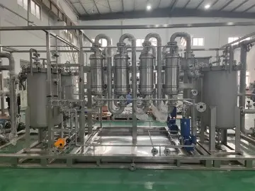
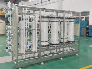
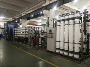
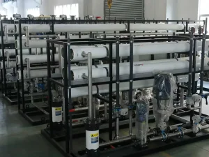
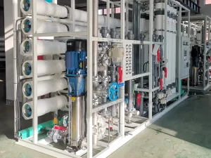
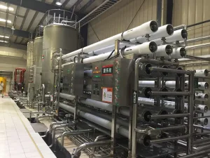
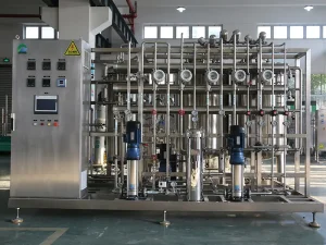
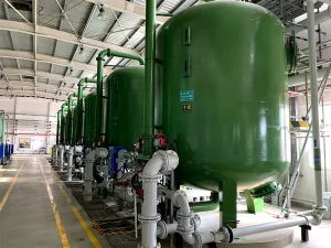
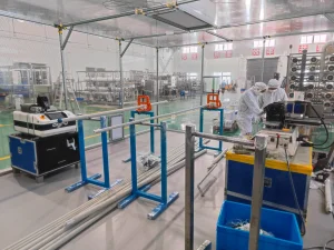
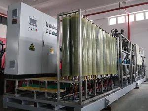
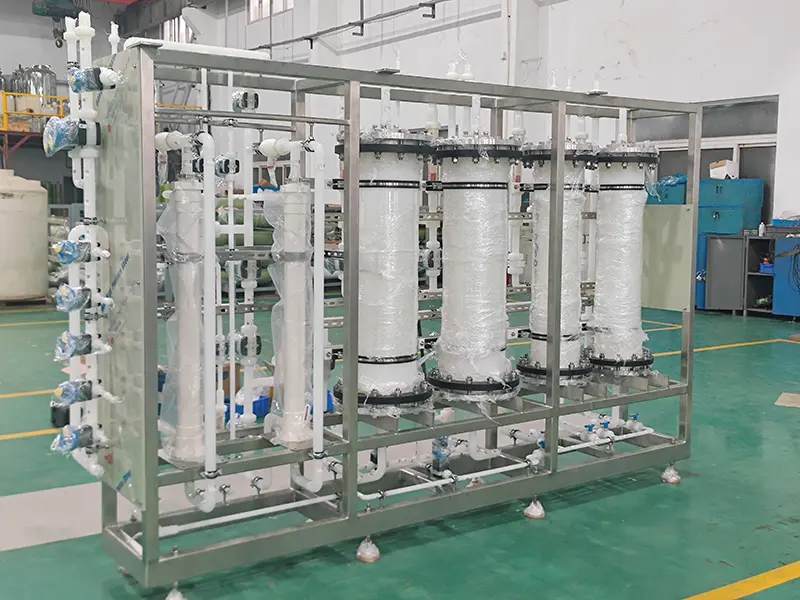
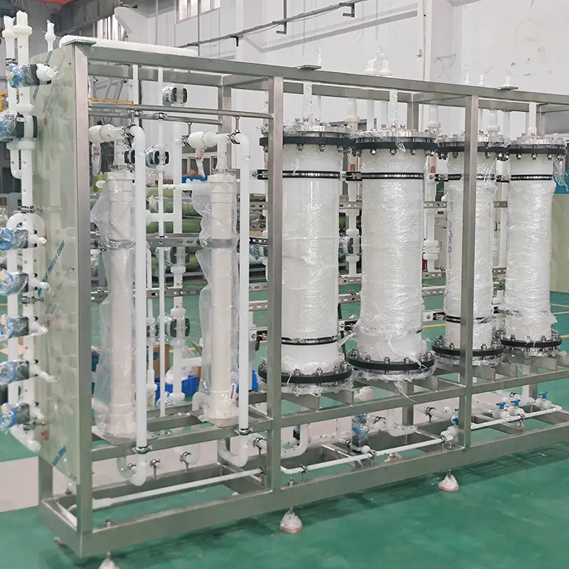
Shanghai Tongjie Environmental Protection provides semiconductor-grade ultrapure water systems employing a comprehensive process flow: pretreatment + two-stage RO + EDI + polishing mixed bed + terminal ultrafiltration + degassing membrane. The produced water exhibits stable resistivity ≥18.2 MΩ·cm (at 25°C), TOC ≤1 ppb, particulate matter ≤0.05 μm, and dissolved oxygen ≤5 μg/L, fully complying with SEMI F57, ASTM E1-2018, and the first-level ultrapure water standard for the electronics industry. Equipped with 316L EP/PVDF high-purity piping, nitrogen-sealed storage tanks, and AIoT intelligent monitoring systems, these systems serve applications in 8–12-inch wafers, advanced packaging, display panels, photovoltaics, and precision electronics manufacturing.
Core Advantages
Excessively high purity
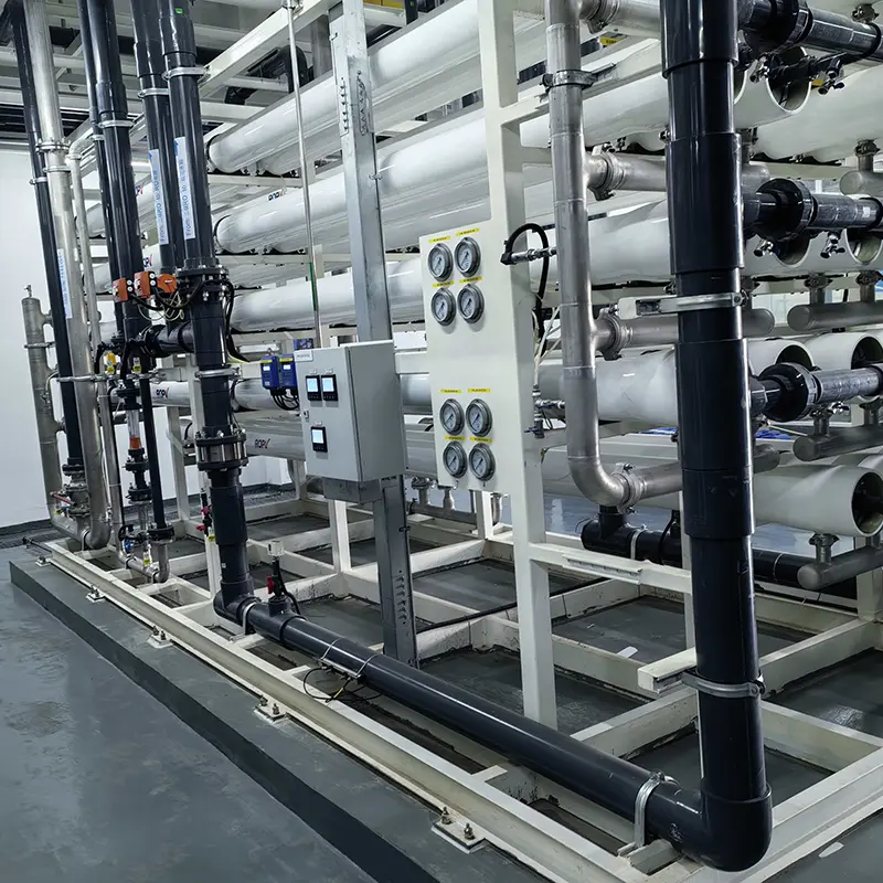
18.2 MΩ·cm stable output from a dual-stage RO+EDI polishing mixed bed, with TOC ≤2 ppb, metal ions
Zero-pollution materials
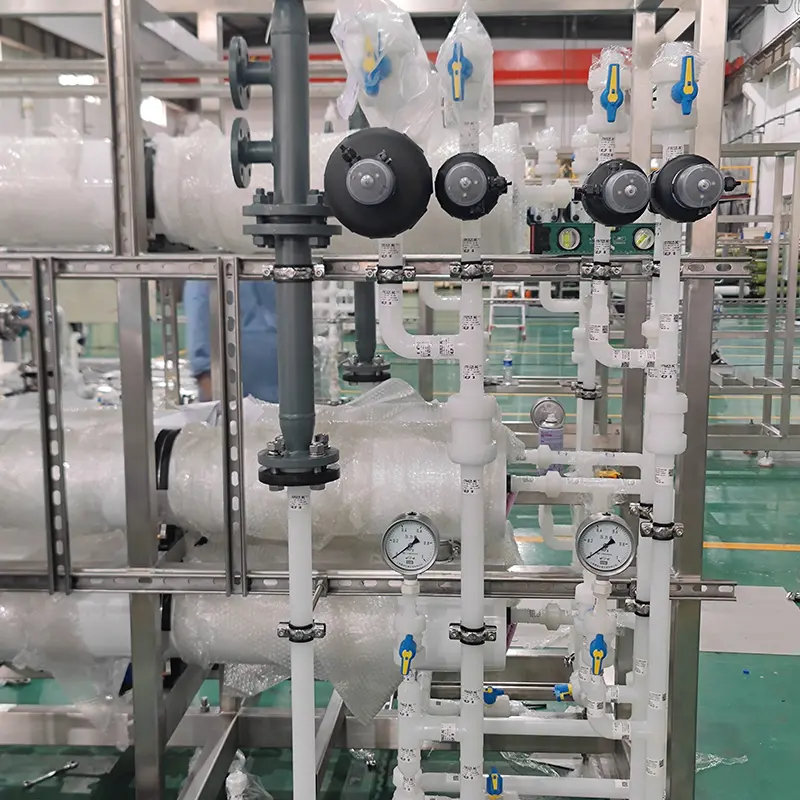
Guaranteed high purity throughout the process using 316L EP stainless steel (Ra ≤ 0.25 μm), PVDF piping, and nitrogen-sealed double-insurance storage tanks.
● Intelligent Monitoring
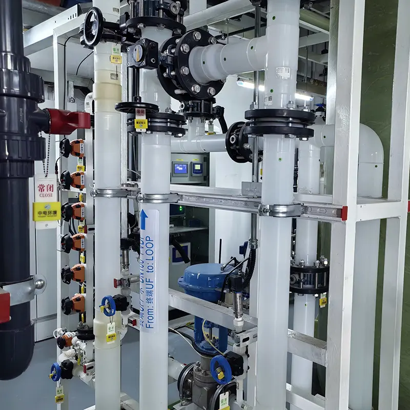
Real-time tracking of 40+ parameters including resistivity, TOC, DO, and metal ions 24/7.
● High Recovery Rate
Energy-saving system achieves ≥85% recovery, reducing energy consumption by 30% per ton.
Application Scenarios
Other Products
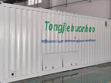
Modular Seawater Desalination
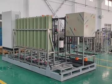
Wastewater & ZLD System
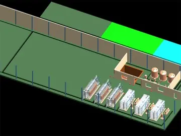
OEM Precision Manufacturing
ODM Full Value Chain Innovation
Water Reuse Equipment (UF+RO)
High-Ratio Water Reuse Process
Industrial Demineralized Water