Direct From Shanghai High-Tech Manufacturing Facility
Engineered Water Treatment & Ultrapure Skid Systems
Explore our pre-assembled, factory acceptance-tested (FAT) membrane separation, desalination, and high-salinity zero liquid discharge assemblies built for mission-critical installations worldwide.
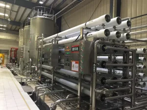
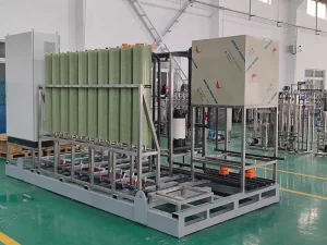
OEM China Suppliers Factory Water Purification System for Food & Beverage Production - Ensuring Safety and Quality Factories, Supplier
OEM China Suppliers Factory Purified Water System for Food & Beverage Production – Ensure Quality and Safety Factories, Suppliers
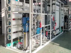
China Compact China Seawater Desalination Equipment by Suppliers - Efficient Reverse Osmosis Factory System for Freshwater Production Factories, Manufacturers
ODM China Food & Beverage Water Purification System - Leading Suppliers & Factory for Safe, Compliant Water Manufacturers, Manufacturer
Wholesale Compact Seawater Desalination System from China Suppliers - Efficient Factory Solutions for Small Freshwater Needs Supplier, Manufacturers
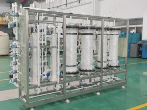
OEM China Suppliers Ultra-Pure Water System for Semiconductor & Electronics Manufacturing | Quality Factory Solutions Factory, Suppliers
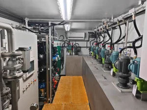
CE Certification Fracturing Flowback Water Reuse Treatment Equipment - China Suppliers & Factory for Oil & Gas Operations Factories, Manufacturer
Technical Whitepaper Depth
Ultrapure Water (UPW) in Semiconductor Fabrication: Physics, Impurity Limits & Process Rigor
In modern microelectronics, water is not merely a utility—it is the highest-volume chemical reagent in direct contact with critical wafer surfaces.
Within sub-10nm and advanced packaging semiconductor foundries, wafer fabrication demands absolute chemical cleanliness. A standard 300mm wafer fabrication plant (fab) processing 40,000 wafer starts per month consumes between 2 to 4 million gallons of Ultrapure Water (UPW) each day. At these physical dimensions, even individual dissolved ions, trace boron, silicates, bacteria, or dissolved gases become fatal yield-killers, causing bridge defects, dielectric breakdown, or lattice contamination.
Ultrapure water reaches the theoretical physical limit of pure H₂O, exhibiting an electrical resistivity of 18.2 MΩ·cm at 25°C. However, resistivity alone no longer guarantees product safety in sub-3nm nodes. Modern procurement specifications dictate stringent microcontaminant thresholds: Total Organic Carbon (TOC) < 0.5 parts per billion (ppb), dissolved oxygen (DO) < 1 ppb, dissolved silica < 0.2 ppb, critical trace metals (such as sodium, iron, and copper) < 0.1 parts per trillion (ppt), and zero bacterial counts per 100 liters.
E-E-A-T Manufacturing Note: Shanghai Tongjie Environmental Protection Technology Co., Ltd. builds membrane separation systems backed by 38+ utility and invention patents. Our modular UPW trains integrate high-flux double-pass RO, vacuum degasification (Liqui-Cel), continuous electrodeionization (CEDI), catalytic 185nm TOC-destruction UV reactors, and PVDF-HP polished piping networks designed specifically for semiconductor cleanrooms.
| Water Quality Parameter | Feed Water Baseline | Standard Industrial Pure Water | ASTM D5127 Type E-1 (Semiconductor) | Tongjie Sub-ppb UPW Spec |
|---|---|---|---|---|
| Resistivity (25°C) | 0.002 - 0.05 MΩ·cm | > 1.0 MΩ·cm | > 18.2 MΩ·cm | 18.24 MΩ·cm (Theoretical Limit) |
| Total Organic Carbon (TOC) | 1,000 - 5,000 ppb | < 200 ppb | < 1.0 - 2.0 ppb | < 0.5 ppb (Dual 185nm VUV) |
| Dissolved Silica (Reactive) | 5,000 - 20,000 ppb | < 50 ppb | < 0.5 ppb | < 0.1 ppb |
| Dissolved Oxygen (DO) | 8,000 - 10,000 ppb | Unregulated | < 1.0 - 3.0 ppb | < 0.8 ppb |
| Particles (> 20 nm) | Millions / mL | < 500 / mL | < 10 / mL | < 1 / mL (UF Polished) |
| Trace Boron | 50 - 500 ppb | < 10 ppb | < 0.05 ppb | < 0.01 ppb (Selective Polishing) |
Localized In-Fab Utilization
Microelectronic Application Scenarios: Where Fab Yields Depend on Water
From wet chemical benches to extreme ultraviolet (EUV) photolithography scanners, UPW interacts with silicon at every step of processing.
Front-End-of-Line (FEOL) RCA Cleaning
Wafer surfaces undergo multiple standard cleans (SC-1 and SC-2) to remove organic residues and metallic particles. UPW is applied as the universal rinsing solvent between aggressive oxidizing and acid etching stages. Any dissolved oxygen in the rinse water can trigger uncontrolled native oxide growth on exposed silicon lattices, compromising sub-gate dielectric thickness.
DO < 1 ppb
SC-1/SC-2 Rinse
Native Oxide Prevention
Chemical Mechanical Planarization (CMP)
CMP planarizes wafer topography via abrasive chemical slurries. Post-CMP scrubbing requires massive volumes of high-velocity UPW to strip silica and ceria slurry particles from microscopic interconnect trenches. Trace ionic contaminants remaining on the polished wafer can generate parasitic capacitance and inter-metal shorts.
Slurry Scrub
Particle Zero-Defect
Cu/W Planarization
EUV & DUV Photolithography Immersion
In 193nm immersion (ArFi) lithography, high-purity water acts as the refractive optical liquid layer between the final lens element and the wafer. The UPW refractive index must remain stable to 10⁻⁶ units. Any micro-bubbles, dissolved air, or organic hydrocarbons cause light scattering, pattern distortion, and critical dimension (CD) variations.
Refractive Precision
Bubble-Free Degas
TOC < 0.5 ppb
Wet Etching & Photoresist Stripping
Following high-aspect-ratio reactive ion etching, harsh stripper chemicals (such as SPM or piranha mixtures) are rinsed with hot ultrapure water. Rinsing 3D NAND deep trench architectures requires surfactant-free water with exceptionally low surface tension to penetrate and flush 100:1 aspect ratios without structural collapse.
3D NAND Flush
Hot UPW (80°C)
High Aspect Ratio
Advanced Packaging & Heterogeneous Chiplets
CoWoS (Chip-on-Wafer-on-Substrate) and 3D stacking require micro-bump solder cleaning and flux removal. Water purity in packaging facilities must now match cleanroom standards to prevent corrosion of micro-bumps spaced below 25-micron pitches.
CoWoS & 2.5D/3D
Micro-Bump Clean
Corrosion Defense
Closed-Loop Fab Wastewater Reclamation
Due to severe municipal discharge constraints and ESG reporting rules, contemporary semiconductor plants reclaim up to 85% of spent rinse water. Tongjie's selective membrane trains treat hydrofluoric (HF), copper-laden, and CMP wastewater streams separately for closed-loop return to the UPW makeup loop.
85%+ Water Reclaim
HF / Heavy Metal Segregation
ESG Fab Benchmark
Sub-Nanometer Engineering Architecture
Process Architecture: The 5-Stage Ultrapure Water Purification Train
Eliminating contaminants to the parts-per-trillion scale requires an orchestrated progression of physical separation, chemical oxidation, and ionic exchange technologies.
01
Pretreatment
Coagulation, multi-media sand/anthracite beds, activated carbon filters, and ultrafiltration (UF) modules lower turbidity, eliminate suspended colloidal matter, and keep the Silt Density Index (SDI₁₅) < 2.5.
02
Primary Demineralization
Two-pass Reverse Osmosis (RO) with energy recovery devices strips > 99.2% of total dissolved solids. High-recovery brackish water membranes reject silica, heavy ions, and raw organics.
03
Continuous Polishing
Continuous Electrodeionization (CEDI) removes trace ionic species without hazardous acid/caustic regeneration, followed by vacuum contactor membranes (Liqui-Cel) to strip DO down to < 5 ppb.
04
VUV TOC Destruction
Dual-wavelength (185nm / 254nm) photochemical reactors generate hydroxyl radicals (•OH) that break carbon chains down to CO₂, which is removed via downstream mixed-bed ion exchangers.
05
Point-of-Use UF Loop
Non-regenerable nuclear-grade ion-exchange resin combined with 6,000 Dalton hollow-fiber ultrafilters eliminates any micro-particles (> 20nm) before pure water enters fab cleanroom loops.
Hydraulic Design & Wetted Material Metallurgy
Constructing a semiconductor UPW delivery network requires strict control of materials in contact with the fluid. Conventional stainless steels leach nickel, chromium, and iron ions when exposed to 18.2 MΩ·cm water, which is chemically aggressive due to its complete ion depletion. Tongjie engineers systems with high-purity Polyvinylidene Fluoride (PVDF-HP) or Perfluoroalkoxy (PFA) for point-of-use cleanroom distribution. Where metallic components are required, we utilize 316L stainless steel with electro-polished inner surfaces (Ra < 0.25 µm), assembled through automated orbital tube welding under high-purity argon shielding.
Manufacturing Capability & Scale
Chinese Manufacturing Ecosystem: Supply Chain Resilience & EPC Delivery Speed
Combining complete vertical integration, rapid modular prefabrication, and proven field engineering to eliminate project schedule overruns.
Historically, fab water infrastructure faced long lead times: European and American engineering houses relied on fragmented subcontractors, resulting in 14- to 20-month delivery schedules. Shanghai Tongjie consolidates mechanical design, pressure vessel fabrication, electrical PLC cabinet wiring, pipe pre-spooling, and clean testing under one ISO 9001/14001/45001-certified factory in Jiading District, Shanghai.
17+
Years Dedicated Engineering Experience
38+
Invention & Utility Model Patents
50+
Specialized Fluid & Mechanical Engineers
1000+
Industrial Installations Across 40+ Nations
Fully Skid-Mounted Modularization
Equipment is built within precision structural steel skids or standard ISO shipping containers. Pre-wired, pre-piped, and factory-tested (FAT), reducing on-site construction schedules from months to weeks.
Integrated Tier-1 Component Sourcing
Direct partnerships with membrane suppliers (DuPont FilmTec, Toray, Hydranautics), Grundfos and Danfoss high-pressure pumps, and Siemens/Schneider automation ensure reliable supply chains.
Cost-to-Performance Advantage
Standardized engineering workflows and local component manufacturing deliver high-spec systems at a 30% to 45% CAPEX savings compared to Western integrators—without compromising component quality.
Global Market Context
Global Fab Expansion & The Water Scarcity Challenge
Navigating the intersection of the US CHIPS Act, European Chips Act, and East Asian mega-cluster builds under stringent environmental regulations.
The semiconductor landscape is experiencing unprecedented geographic redistribution. Billions in public and private capital are pouring into wafer fabs across Arizona, Texas, Dresden, Kumamoto, Singapore, and across China. However, a major bottleneck to fab operational readiness remains water infrastructure and watershed permitting.
A leading 3nm foundry in a water-stressed basin can consume municipal water equivalent to a city of 150,000 residents. During regional droughts, municipal authorities restrict intake quotas. Fab operators must turn to seawater desalination intake (for coastal facilities in Japan and Southeast Asia) or high-recovery Zero Liquid Discharge (ZLD) reclamation. Tongjie's containerized seawater RO systems and disc-tube RO (DTRO) assemblies allow fabs to secure private water supplies, insulate production from regional grid curtailments, and reclaim high-salinity wastewater streams for ongoing reuse.
International Certification
Strict Global Compliance: SEMI F63, ASTM & Electrical Directives
Every UPW system shipped from Shanghai Tongjie meets international cleanroom safety and electrical conformity standards.
SEMI Standards Compliance
Engineered to SEMI F63-0213 (Guide for Ultrapure Water Used in Semiconductor Processing) and SEMI F75 (Guide for Quality Monitoring of Ultrapure Water Used in Semiconductor Manufacturing). All piping loops prevent dead legs (L/D < 3).
CE, ASME & UL Electrical Directives
All pressure vessels are fabricated to ASME Section VIII / PED specs. Electrical cabinets are built to CE directives and NFPA 79 / UL 508A specifications with dual-safety circuit interlocks and multi-language HMI interfaces.
Digital Twin & Remote Telemetry
Integrated SCADA with IoT gateways provides real-time tracking of individual sensor nodes (resistivity, DO, TOC, pressure drops). Predictive alerts notify technicians of membrane scaling weeks before delta-P breaches occur.
Purchasing & Engineering FAQ
Frequently Asked Questions on Wholesale Semiconductor UPW Systems
Key technical and commercial queries from EPC contractors, facility directors, and procurement leaders.
How does Tongjie achieve TOC levels below 0.5 ppb for semiconductor wet chemistry?
Achieving TOC < 0.5 ppb requires a multi-stage destruction mechanism. We position high-intensity 185nm / 254nm dual-wavelength vacuum ultraviolet (VUV) reactors downstream of primary demineralization. The 185nm photolysis splits H₂O molecules into highly reactive hydroxyl radicals (•OH), which oxidize organic compounds into charged carbonate and CO₂ species. These oxidized ionic molecules are then trapped by downstream virgin, non-regenerated nuclear-grade mixed-bed polishers.
Why is boron removal challenging in UPW, and how do your systems address it?
Boron predominantly exists as uncharged boric acid (H₃BO₃) at neutral pH, passing easily through standard RO membranes. Because boron acts as a p-type dopant in silicon, even 0.05 ppb can alter semiconductor resistivity. Tongjie applies chemical pH adjustment (dosing pure NaOH into the second-pass RO feed to shift pH > 9.5). At this basic pH, boric acid dissociates into ionized borate (H₂BO₃⁻), enabling the second RO pass to reject over 98% of boron before passing through selective ion-exchange resin.
What is the standard lead time for a containerized industrial or UPW system?
Standard containerized systems (e.g., containerized SWRO, pure water skids, and DTRO produced water units) carry an engineering-to-FAT lead time of 8 to 12 weeks. Fully custom, multi-train semiconductor UPW installations spanning cleanroom PVDF loops generally deliver within 16 to 24 weeks—well ahead of typical 12- to 18-month lead times from traditional Western systems integrators.
Can Tongjie equipment integrate with existing plant Distributed Control Systems (DCS)?
Yes. Our standard automation platforms use Siemens S7-1500 or Allen-Bradley ControlLogix PLCs with industrial Ethernet communication protocols including Profinet, Modbus TCP/IP, and EtherNet/IP. We provide complete electrical schematics, I/O lists, control narratives, and functional design specifications (FDS) for seamless integration with fab-wide SCADA systems.
How are sanitary conditions maintained within the UPW cleanroom distribution loop?
To prevent biofilm formation, distribution systems maintain continuous turbulent flow (velocities > 1.5 to 2.0 m/s) with zero dead-legs throughout the piping infrastructure. The loop integrates continuous 254nm germicidal UV irradiation and periodic automated hot water sanitization (80°C to 85°C) across PVDF-HP piping, eliminating the need for chemical sanitizing agents that require extensive rinse-down cycles.
What documentation packages are supplied for validation and quality audits?
Every system includes comprehensive documentation: Factory Acceptance Testing (FAT) records, Material Test Reports (MTRs) with 3.1 mill certs, weld maps and endoscopic inspection logs, surface roughness (Ra) profilometer certifications, instrument calibration certificates, operational and maintenance manuals, and complete spare parts catalogs.
Specialized Heavy Industrial & ZLD Equipment Lines
High-Salinity, Water Reuse & Pharmaceutical Grade Product Solutions
Complete fluid handling lines: oilfield fracturing flowback treatment, high-pressure membrane concentration, and API pharmaceutical systems.
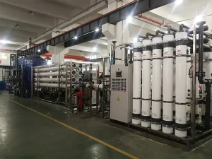
Wholesale High-Ratio Water Reuse Equipment from China Suppliers - Advanced Pretreatment, UF, and RO Factory Solutions Factory, Manufacturer
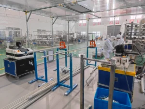
China Eco-Friendly Water Treatment Solutions: ODM Services by China Suppliers & Factory for Global Brands Suppliers, Supplier
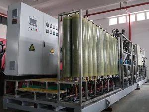
CE Certification China Fracturing Flowback Fluid Treatment System by Suppliers and Factory for Zero-Discharge Reuse Factory, Suppliers
Wholesale China Suppliers Factory for Oilfield Fracturing Flowback Fluid Treatment System - Zero Discharge Solution Suppliers, Manufacturer
ODM China Food & Beverage Process Water System - Reliable Suppliers and Factory Solutions for Purified Water Factory, Manufacturers
China High-Ratio Water Reuse Equipment in China - Suppliers and Factory for Pretreatment, UF, and RO Process Suppliers, Supplier
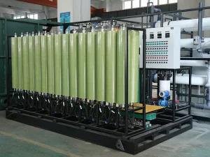
ODM High-Pressure Membrane Concentration System for High-Salinity Wastewater - China Suppliers & Factory Solutions Factories, Manufacturers
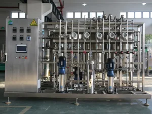
Wholesale China Pharmaceutical Purified Water & WFI System Suppliers - High-Quality Factory Solutions for APIs Factories, Manufacturers
Request an Engineered Process Simulation & Proposal
Submit your raw water chemistry analysis, flow volume requirements, and cleanroom target specifications. Our senior fluid engineers will prepare a complete mass-balance schematic, P&ID layout, and detailed equipment quote within 48 business hours.